PWM is used in all sorts of power control and converter
circuits. Some examples we have are motor control, DC-DC converters, DC-AC
inverters and lamp dimmers. . One of the most popular of such
controllers is the versatile and ubiquitous SG3525
SG3525 is used extensively in DC-DC converters, DC-AC
inverters, home UPS systems, solar inverters, power supplies, battery chargers
and numerous other applications.
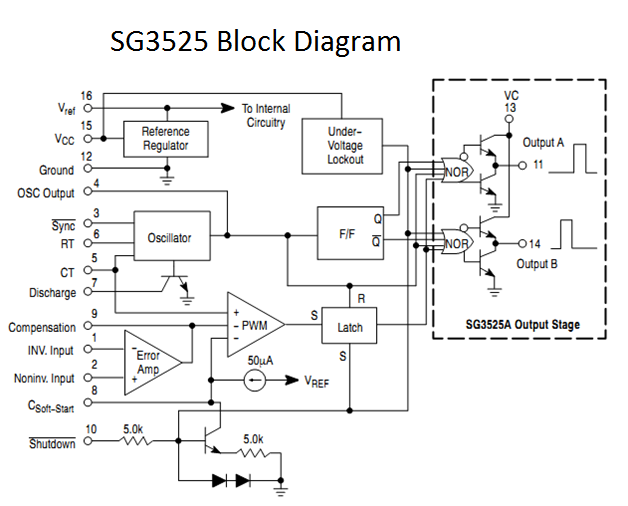
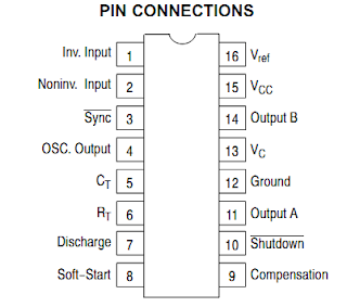
let’s just look at the block diagram and the pin layout.of sg3525 ic
Pins 1 (Inverting Input) and 2 (Non Inverting Input) This functions either to increase or decrease the duty cycle
depending on the voltage levels on the Inverting and Non-Inverting Inputs –
pins 1 and 2 respectively.
- When
voltage on the Inverting Input (pin 1) is greater than voltage on the
Non-Inverting Input (pin 2), duty cycle is decreased.
- When
voltage on the Non-Inverting Input (pin 2) is greater than voltage on the
Inverting Input (pin 1), duty cycle is increased.
The frequency of PWM is dependent on the timing capacitance
and the timing resistance. The timing capacitor is connected between pin 5
and ground. The timing resistor is connected between pin 6 and ground. The
resistance between pins 5 and 7 (RD) determines the deadtime
The frequency is related to RT, CT and RD by the
relationship:
With RT and RD in Ω and CT in F, f is in Hz.
Typical values of RD are in the range 10Ω to 47Ω. The range
of values usable (as specified by the manufacturers of SG3525) is 0Ω to 500Ω.
RT must be within the range 2kΩ to 150kΩ. CT must be within
the range 1nF (code 102) to 0.2µF (code 224). The oscillator frequency must be
within the range 100Hz to 400kHz. There is a flip-flop before the driver stage,
due to which your output signals will have frequencies half that of the
oscillator frequency that is calculated using the above mentioned formula. So,
if you are looking to use this for a 50Hz inverter, you require drive signals
of 50Hz. So, the oscillator frequency must be 100Hz.
A capacitance connected between pin 8 and ground provides
the soft-start functionality. The larger the capacitance, the larger the
soft-start time. This means that the time taken to go from 0% duty cycle to the
desired duty cycle or maximum duty cycle is larger. So, the duty cycle
increases more slowly initially. Keep in mind that this only affects initial
rate of increase of duty cycle, ie, the rate of increase of duty cycle after
the SG3525 starts up.
Typical values of the soft-start capacitance lie within the
range 1µF to 22µF depending on the desired soft-start time.
Pin 16 is the output from the voltage reference section.
SG3525 contains an internal voltage reference module rated at +5.1V that is
trimmed to provide a ±1% accuracy. This reference is often used to provide
a reference voltage to the error amplifier for setting the feedback reference
voltage. It can be directly connected to one of the inputs or a voltage divider
can be used to further scale down the voltage.
Pin 15 is VCC – the supply voltage to the SG3525 that makes
it run. VCC must lie within the range 8V to 35V. SG3525 has an under-voltage
lockout circuit that prevents operation when VCC is below 8V, thus preventing
erroneous operation or malfunction.
Pin 13 is VC – the supply voltage to the SG3525 driver
stage. It is connected to the collectors of the NPN transistors in the output
totem-pole stage. Hence the name VC. VC must lie within the range 4.5V to 35V.
The output drive voltage will be one transistor voltage drop below VC. So when
driving Power MOSFETs, VC should be within the range 9V to 18V (as most Power
MOSFETs require minimum 8V to be fully on and have a maximum VGS breakdown
voltage of 20V). For driving logic level MOSFETs, lower VC may be used. Care
must be taken to ensure that the maximum VGS breakdown voltage of the MOSFET is
not crossed. Similarly when the SG3525 outputs are fed to another driver or
IGBT, VC must be selected accordingly, keeping in mind the required voltage for
the device being fed or driven. It is common practice to tie VC to VCC when VCC
is below 20V.
Pin 12 is the Ground connection and should be connected to
the circuit ground. It must share a common ground with the device it drives.
Pins 11 and 14 are the outputs from which the drive signals
are to be taken. They are the outputs of the SG3525 internal driver stage and
can be used to directly drive MOSFETs and IGBTs. They have a continuous current
rating of 100mA and a peak rating of 500mA. When greater current or better
drive is required, a further driver stage using discrete transistors or a
dedicated driver stage should be used. Similarly a driver stage should be used
when driving the device causing excessive power dissipation and heating of
SG3525. When driving MOSFETs in a bridge configuration, high-low side drivers
or gate-drive transformers must be used as the SG3525 is designed only for
low-side drive.
Pin 10 is shutdown. When this pin is low, PWM is enabled.
When this pin is high, the PWM latch is immediately set. This provides the
fastest turn-off signal to the outputs. At the same time the soft-start
capacitor is discharged with a 150µA current source. An alternative method of
shutting down the SG3525 is to pull either pin 8 or pin 9 low. However, this is
not as quick as using the shutdown pin. So, when quick shutdown is required, a
high signal must be applied to pin 10. This pin should not be left floating as
it could pick up noise and cause problems. So, this pin is usually held low
with a pull-down resistor.
Pin 9 is compensation. It may be used in conjunction with
pin 1 to provide feedback compensation.


No comments:
Post a Comment